Capabilities Parameters
-
Material
High Tg, FR-4 -
Number of Layers
Rigid(1~40) -
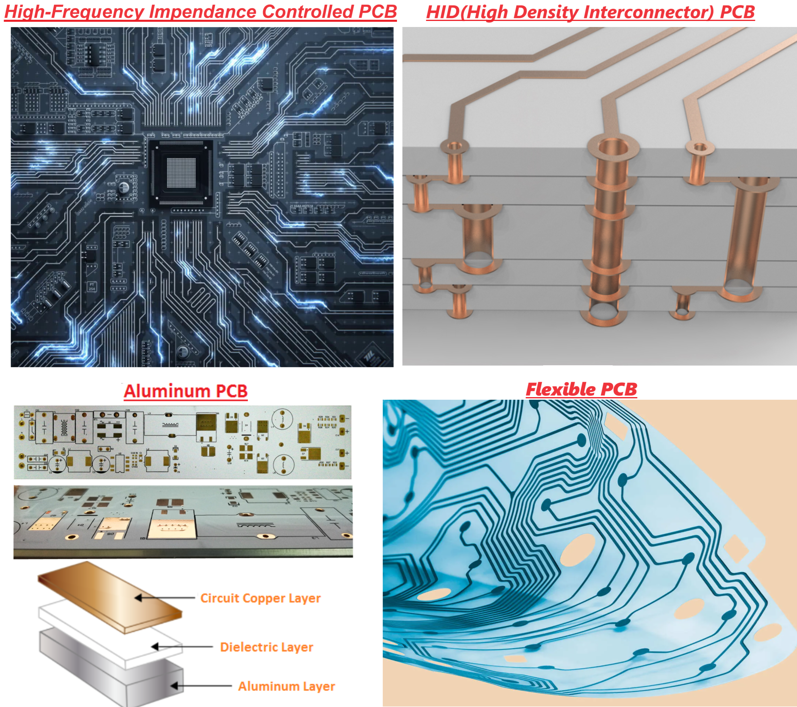
HDI and others
HDI (1~3 steps) | R-FPC (2-16 layers) -
PCB size(Finished)
Max: 24"*24", Min: 0.2"*0.2" -
Internal Layer thickness(Min.)
1/3 OZ (12um) -
External Layer thickness(Max.)
6 OZ (216um) -
Min. width/gap (Int)
2.5/3mil (H/H OZ base copper) -
Min. width/gap (Ext)
3/3mil (H/H OZ base copper) -
Min. gap between hole wall and conductor(Int):
6 mil -
Min. gap between hole wall and conductor(Ext):
6 mil -
Min. annular ring for throng hole
3 mil -
Min. annular ring for IC Pads
5 mil -
Min BGA Pad
8 mil -
Min. BGA Pitch
0.4mm -
Min finish hole DIA
0.15mm(CNC) 0.1mm(Laser) -
Max aspect ratio
20:1 -
Min SM bridge for solder mask
3 mil -
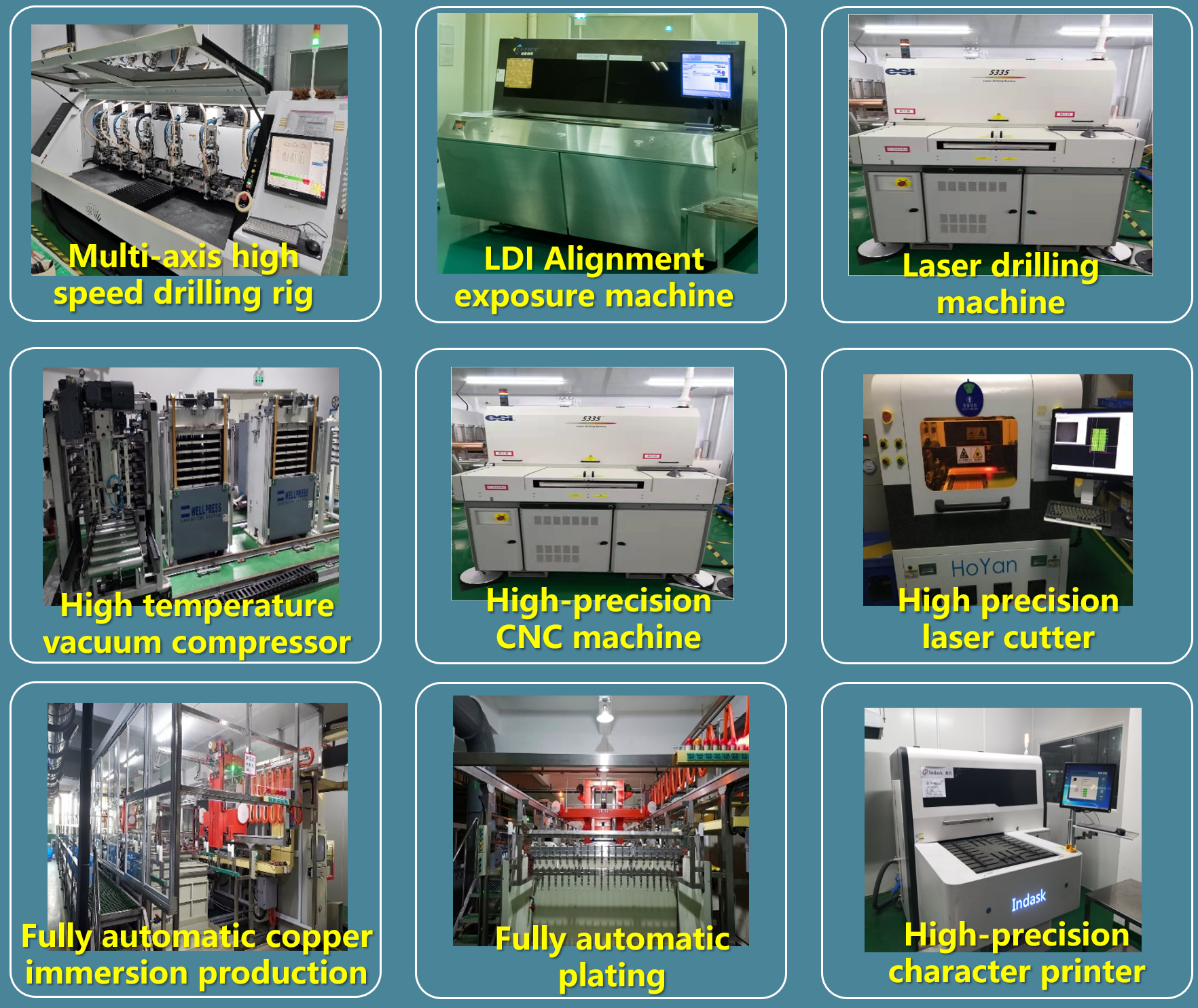
Solder mask / line processing method
Film/Laser etching -
Min Insulation thickness
2 mil -
Finish treatment
Immersion Gold,Tin,Silver,Lead Free HASL,Plating Gold